FPGA overview 10AX016 10AX022 10AX027 10AX032 Logic elements (LEs) 160K 220K 270K 320K Adaptive logic modules (ALMs) 61,510 83,730 101,620 118,730 ALM registers 246,040 334,920 406,480 474,920 M20K memory blocks 440 588 750 891 M20K memory size (Mb) 9 11 15 17 MLAB memory size (Mb) 1.0 1.8 1.8 2.4 2.8 Variable-precision digital
signal processing (DSP) blocks156 191 830 985 18 x 19 multipliers 312 382 1,660 1,970 Peak fixed-point peformance (GMACS) 343 420 1,826 2,167 Peak floating-point performance (GFLOPS) 140 172 747 887 Maximum user I / O pins (Device) 288 288 384 384 Maximum user I / O pins (Board) 128 128 128 128 For more information on FPGA overview, please visit the Intel Arria 10 GX website.
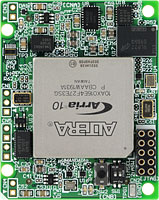
- Equipped with Intel Arria 10 GX FPGA
- 10AX016E4F27E3SG
- 10AX022E4F27E3SG
- 10AX027E4F27E3SG
- 10AX032E4F27E3SG
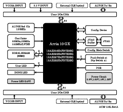
- 3.3V single power supply 1.8V, 0.9V, 1.03V, 1.35V are generated in the board
* I / O power supply (VCCOA / VCCOB) must be supplied from CNA and CNB. - Configuration ROM: MT25QU256
- Onboard clock: 50MHz, 100MHz (CMOS), 100MHz (LVDS)
can be supplied externally - High-speed transceiver Evaluable
Tx / Rx pair is pulled out to each connector (CNA / CNB) and
equipped with a reference clock (125MHz) - Equipped with
DDR3L SDRAM (Micron, 4Gbit ) MT41K512M8DA-107: P (512M x 8) - JTAG connector
download cable
Compatible with various USB Blaster, etc. 10-pin socket - General purpose LED x2
- General-purpose switch x2
Push button switch x1
DIP switch x1 - Status LED: CONF_DONE (blue), POWER LED (red)
- Equipped with a reset circuit for configuration
- User I / O: 128 (CNA: 64 / CNB: 64) The
CNA and CNB I / O power supplies (VCCOA / VCCOB) are separated and must be supplied from the outside. It supports voltages up to 1.2V, 1.25V, 1.35V, 1.5V, 1.8V.CNA CNB A board IOA0-63:
MAX 25.7mm
MIN 21.6mmIOB0-63:
MAX 21.2mm
MIN 17.1mm- Not all I / O is LVDS compatible
- Users are requested to consider each I / O standard based on FPGA materials.
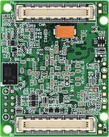
- 10-layer board
- Board dimensions: 54mm x 43mm half card size


