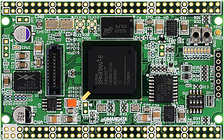
■ Equipped with XC6SLX45T-2FGG484C, XC6SLX75T-2FGG484C
FPGA overview Spec XC6SLX45T XC6SLX75T XC6SLX100T XC6SLX150T Slices 6,822 11,662 15,822 23,038 Logic Cells 43,661 74,637 101,261 147,443 Maximum Distributed RAM (Kb) 401 692 976 1,355 Total Block RAM (Kb) 2,088 3,096 4,824 4,824 Maximum user I / O pins (Device) 296 348 498 540 Maximum user I / O pins ( Board ) 100 100 100 100 DCMs 8 12 12 12 PLLs Four 6 6 6 DSP Slices 58 132 180 180
XC6SLX100T-2FGG484C or XC6SLX150T-2FGG484C
■ Abundant I / O extraction (100)
■ Onboard clock 30MHz
, 50MHz (LVTTL)
■ Configuration SPI-ROM
Micron: M25P64 iMPACT ISP possible from
■ DDR2 SDRAM
Micron: MT47H32M16HR-25E: G, 512Mbit
■ MRAM installed ( Note : not installed in
75T)Everspin: MR2A16AYS35, 4Mbit
■ RocketIO evaluable TX / RX 4ch each ( SIF40 connector )
( 125MHz , 150MHz , Reference clock installed, external input possible (MMCX))
125 / 150MHz and communication standard
■ 7-pin JTAG connectorEquipped
FPGA configuration
Configuration SPI-ROM ISP
■ 3.3V single power supply operation
1.2V, 2.5V, 1.8V, 0.9V generated in board
■ 8 general-purpose LEDs
■ 4 general-purpose switches
Push button switch x2
DIP switch x2
■ Separate VCCO (part of CNB) (Tested at 3.3V at the time of manufacture)
■ VREF input possible (CNB) (Not tested at the time of manufacture)
■ Reset function for configuration
■ Adopted 8-layer board
■ I Wiring length control of / O (memory is managed separately)
■ Credit card size 54mmX86mm RoHS directive compliant


