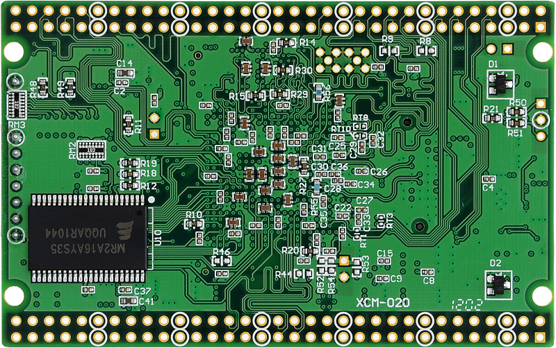
FPGA overview XC7A200T Logic Cell 215,360 Slice 33,650 Max Distributed RAM (kb) 2,888 Max Block RAM (kb) 13,140 DSP Slice 740 CMT (MMCMx1+PLLx1) Ten GTP Channel (Device) 16 GTP Channel ( Board ) Four Max user I/O (Device) 500 Max user I/O ( Board ) 296 For details of the FPGA outline, see the page of XILINX Artix-7 .
- Equipped with XC7A200T-1FFG1156C
- User I/O: 296 pcs
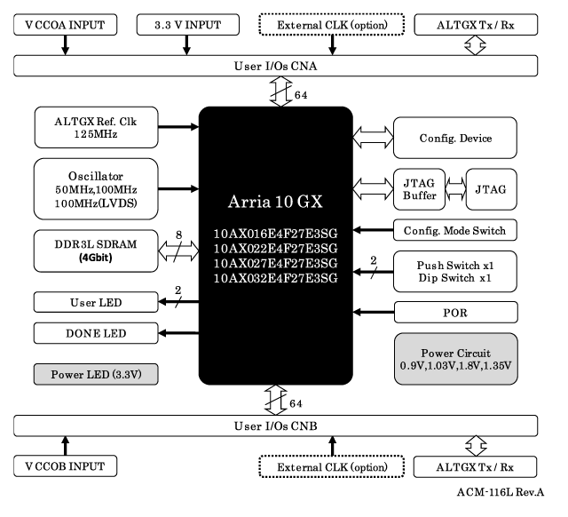
IOA (CNA connector): 64 pcs Vcco = 3.3V
IOB (CNB connector): 64 pcs Vcco = External input
IOC (CNC connector): 84 pcs Vcco = External input
IOD (CND connector): 84 This Vcco = External inputIOA IOB IOC IOD A board MAX
40.4mm MIN 25.5mmMAX 34.2mm
MIN 24.7mmMAX 46.8mm
MIN 27.2mmMAX 50.6mm
MIN 23.1mm- Not all I/Os are LVDS capable
- Please consider each I/O standard by the user based on FPGA materials etc.
- 3.3V single power supply operation
1.0V, 1.2V, 1.5V, 1.8V, 2.5V are generated on the board
Power supply sequencer installed (at the time of turning on ) - RocketIO (GTP) evaluation possible
CNA/CNB to TX/RX 2ch each, total 4ch
reference clock: 125MHz(LVDS), external input possible (MMCX)
DDR4 SDRAM installed MT41K64M16 (Micron, 1Gbit) 4Gbit
possible by custom order- Configuration ROM
MT25QL128ABA1ESE-0SIT (Micron, 128Mbit) - On-board clock
50MHz (LVTTL), 200MHz (LVDS)
can be supplied externally - General-purpose LED x2
- General-purpose switch x2
Push button x1
Dip switch x1bit - 7-pin JTAG connector equipped
configuration of the FPGA
ISP to the configuration ROM
in the JTAG Buffer circuit, realize the download stable - Status LED: CONF_DONE (blue), POWER LED (red)
- Built-in reset circuit for configuration
- 10 layer board
- Board size: 54mm x 86mm Credit card size
- RoHS compliant
 RoHS compliant
| How to use 7-pin JTAG connector for XILINX |
| → |
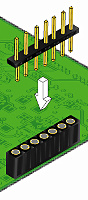

The JTAG connector is a socket. Please mount the pin header when using.
(The socket we use is not a general round pin socket, but a 0.64 mm square pin)
- Block Diagram